
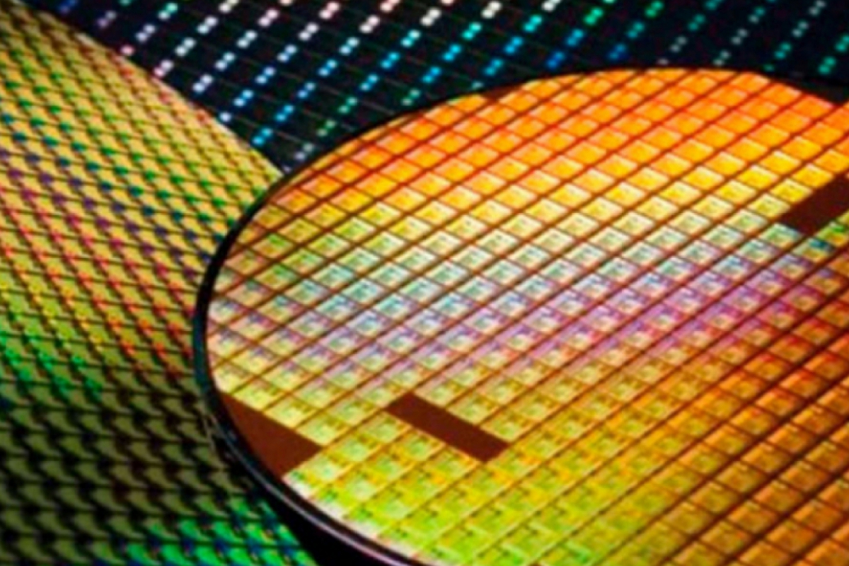
TSMC manages to make 2 Nm memory chips with a 90% yield
The development of the TSMC 2 nanometers process seems to be the stern wind, according to the latest reports and rumors of the company’s environment, the company would have reached a yield above the 90% in the manufacture of memory chips to 2 nanometers.
A 90% yield It means that in each wafer made of 2 nanometers, 90% of the chips are functional. It is, therefore, an impressive performance, especially if we take into account that at direct competence, Samsung was costing him to exceed 20 %. However, it must be taken into account that it is not the same to manufacture memory chips than much more complex chips such as CPUS or GPUS, and the performance of the production of different types of chips is not comparable.
According to the reports, TSMC is receiving four times more chips designs to manufacture 2 nanometers than those I received when it was in the 5 nanometers. This high demand will be accompanied, possibly, an increase in prices.
Additionally, it seems that TSMC facilities in Arizonaat least those that are already built, are also reaching their maximum production capacity with orders from companies such as NVIDIA or Apple. In these facilities the company only has allowed to manufacture 4 and 5 nanometers by restrictions of the Taiwan government itself.