
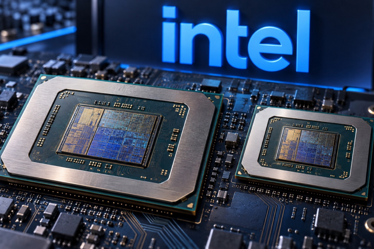
Images of the Intel Nova Lake-HX and H are filtered: this is how their 28 and 16 cores would be distributed
The first images attributed to the interior of the future Intel Nova Lake-HX and Nova Lake-H allow you to compare two laptop configurations. The largest is labeled with eight performance cores, 16 efficiency and four low consumption cores: 28 in total. The second reduces the first two groups to four and eight cores, respectively, and retains four low-power ones. The result would be 16 cores for Nova Lake-H.
The material comes from a leak and not from an Intel technical presentation. It includes measurements and names of manufacturing processes for each block, but does not yet confirm that they correspond to the definitive commercial chips. It also does not reveal frequencies, consumption, cache or specific models. The novelty is in the proposed physical distribution and in the size differences between the two mobile versions.
Nova Lake-HX would occupy 360 mm² and reserve 104 mm² for the calculation
The image attributed to Nova Lake-HX shows a 12 × 30 mm encapsulation, equivalent to 360 mm2 of surface. Inside there are four functional blocks and two other pieces without active logic, used to complete the structure. The encapsulation surface should not be confused with the silicon surface that performs calculations: it includes the areas occupied by these auxiliary parts and the space necessary to assemble the modules.
The main calculation block would be 104 mm2. According to the leak labels, it integrates eight P cores and 16 E cores and uses TSMC’s N2P process. Next to it appears an 85 mm² piece identified as a structural element. If this distribution is correct, the module with the most cores occupies less than a third of the total surface of the package; the rest is divided between graphics, drivers, low-power cores and physical support.
The manufacturing attributed to TSMC refers to that specific block, not the entire processor. In a modular design, parts can be manufactured at different nodes and then assembled into a single package. The images map other parts to Intel processes. There is no independent confirmation of the provenance of each piece or the costs that this combination would entail.
The low-power cores would be in a central block
The proposal places the four LP-E cores in a 72 mm2 center block. The label attributes the Intel 18A-P node. On one side would be located another 58 mm2 module for peripheral control functionsalso identified with Intel 18A-P. Separating these elements from the calculation block explains why the number of cores in the main module, 24 in the HX case, is lower than the 28 total cores indicated for the processor.
The graphics section would use a 26 mm2 block with four Xe cores and the Intel 3-E processalways in accordance with the filtered annotations. That both models share that block in the images does not mean that all mobile Nova Lakes will have exactly the same GPU. A different configuration might require another module, and a part present in a schematic also does not demonstrate that all its resources are activated in each commercial product.
The two auxiliary parts have a different function than the CPU or GPU. They appear as structural filler blocks to complete the package and maintain the arrangement of the other components. They should not be added as additional cores or interpreted as cache without supporting documentation. Its presence also helps to understand why the size of the package does not decrease in the same proportion as the number of calculation cores.
Nova Lake-H would reduce the computing block to 55 mm²
The H variant would have a 12 × 23 mm package, that is, 276 mm2. The main block would be reduced to 55 mm2 and would integrate four P and eight E cores. The four LP-E would remain in the central block, so the announced figure for this configuration would be 16 cores. The images maintain the areas of 26 mm2 for graphics, 72 mm2 for the central block and 58 mm2 for peripheral control.
The main difference between H and HX would, therefore, be in the piece that houses the P and E nuclei and in the structural space that accompanies it. The calculation module of the H version would occupy 49 mm2 less than that attributed to HX. The complete package would be 84 mm2 smaller. Those figures describe physical sizes; By themselves they do not allow us to deduce performance, efficiency or price.
The distribution also leaves open questions. The images do not specify supported memory, connection speeds, cache capacity, or core behavior under sustained load. In a laptop, the final performance will also depend on the power and cooling limits chosen by each manufacturer. None of those elements can be measured from a photograph of the silicon.
Intel has not yet announced the Nova Lake-H and HX with a commercial listing. The images point to a version with 28 cores and another with 16, but their design, manufacturing processes and sizes are still pending official confirmation. There is also no sale date or specific equipment linked to these two configurations.
