
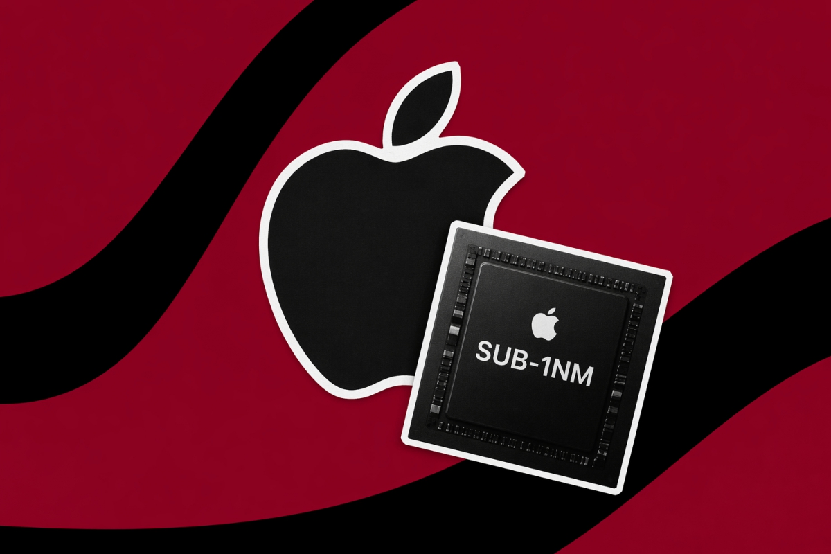
Apple could debut sub-1 nm chips as early as 2029 if TSMC meets its new roadmap
TSMC is already looking beyond 2 nanometers. According to information published by DigiTimes and collected by wccftechthe Taiwanese foundry would be preparing the trial production of a sub-1 nm process in 2029a movement that marks the next big leap for the industry and once again places Apple as a natural candidate to debut this technology in a commercial product.
The roadmap attributed to TSMC fits with the calendar that is already being managed for its most advanced nodes. The first 2nm chips should arrive later this year, with Apple among the customers best placed to adopt them in its upcoming mobile SoCs. From there, the manufacturer would also plan to take its process to mass production. 1.4nm A14 in 2028before making the leap to an even more ambitious sub-nanometer generation.
The most striking fact in the report is that TSMC would have set an initial goal of 5,000 wafers monthly for that early phase of the sub-1 nm process. To do this, it would use several facilities, including the A10 complex in Tainan and plants identified as P1 to P4. We are not yet facing large-scale commercial production, but rather an industrial validation phase that will serve to measure performance, stability and costs in a much more demanding node than the current ones.
Apple once again appears as the most logical candidate
Although the report does not cite specific clients for this future lithography, Apple is once again the name that makes the most sense in this scenario. The company has been operating for years as one of the early adopters of TSMC’s most advanced nodesespecially in chips for iPhone, iPad and Mac. Likewise, it usually absorbs a good part of the initial capacity in exchange for paying a premium to ensure preferential supply.
This is already being seen with the transition to 2nm, where several large chip designers are expected to coincide in very similar windows. In the race for 2 nm, Apple, Qualcomm and MediaTek already appear as candidates to launch this new generation, something that increases pressure on TSMC at a time when demand for cutting-edge capacity continues to grow.
The problem is that the node jump does not depend only on the calendar, but on the yield, that is, the percentage of valid chips obtained per wafer. That is precisely one of the points that will mark the future of this technology. TSMC had already achieved positive signals with previous processes, to the point that it reached a yield of 60% at 2 nm, but going below that barrier requires even greater complexity in materials, lithography and manufacturing costs.
More power and efficiency, but also more pressure on prices and ranges
On paper, TSMC promises improvements of up to 30% in performance and energy efficiencyan especially valuable combination in mobile phones and laptops, where each node jump allows you to gain autonomy or maintain power in more controlled thermal envelopes. Sub-1 nm should push this trend even further, although talking about specific figures today would be premature.
There is also a less optimistic reading. The tighter the node becomes, the more expensive and complex it is to manufacture, and that can translate into more limited adoption during the first few generations. In fact, speculation is already circulating about manufacturers that could reserve their most advanced chips only for Ultra models or premium variants, leaving the rest of the catalog with less cutting-edge versions to contain costs.
Therefore, more than an immediate product promise, this move by TSMC works as a sign of where the industry is headed. If the schedule holds, Apple could be one of the first to benefit from a new jump below the nanometer. But before we get there, the big test will be to see if TSMC can convert that technical ambition into real industrial capacity without the price skyrocketing even further.