Intel 18A-P is now in production: up to 9% more performance and 18% less consumption
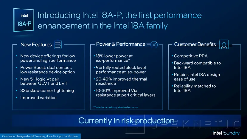
Intel has taken advantage of the VLSI Symposium 2026 to update the status of its upcoming manufacturing processes, with Intel 18A-P as the main protagonist. The Intel 18A-P process, which is an evolution of 18A, is already has entered into risk productiona step prior to mass manufacturing that allows the process to be validated with real designs and prepare for their arrival to clients and products.
The Intel 18A-P is presented as the first performance improvement within the Intel 18A family, the node with which Intel introduced key technologies such as gate-all-around transistors and PowerVia power. According to data shared by the company, Intel 18A-P offers up to 9% more performance at the same consumption or up to 18% less consumption at the same performance compared to Intel 18A. These figures have been obtained by trying to produce an ARM core common in the industry, according to Intel itself.
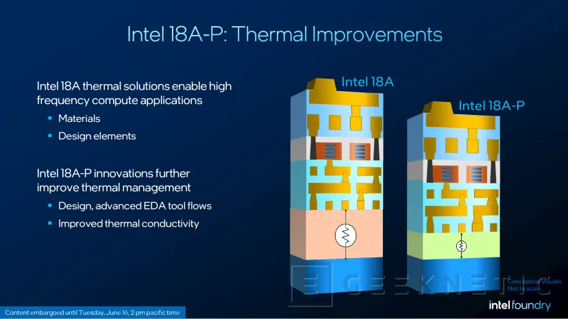
The improvement is not just limited to raw performance. Intel also talks about a reduction of between 20% and 40% in thermal resistance, as well as an improvement of between 10% and 30% in the resistance of the critical paths, the vertical connections that communicate the different layers of the chip. These are important changes because as advanced nodes reduce dimensions and increase density, thermal dissipation and interconnections become bottlenecks as relevant as the transistor itself.
One of the most notable technical innovations of the Intel 18A-P is what they call “Power Boost”, a new low-resistance transistor-based option that makes double contact. This configuration combines front contact and direct rear contact, taking advantage of the PowerVia infrastructure to increase driving current and improve frequency. With this, Intel seeks to extract more performance without disproportionate penalties in consumption or area.
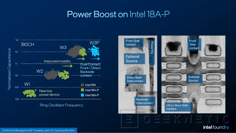
Intel has also introduced new transistor options aimed at both low power and high performance. Additionally, the process allows granularity for chip developers to adjust the balance between frequency, consumption and electrical leakage.
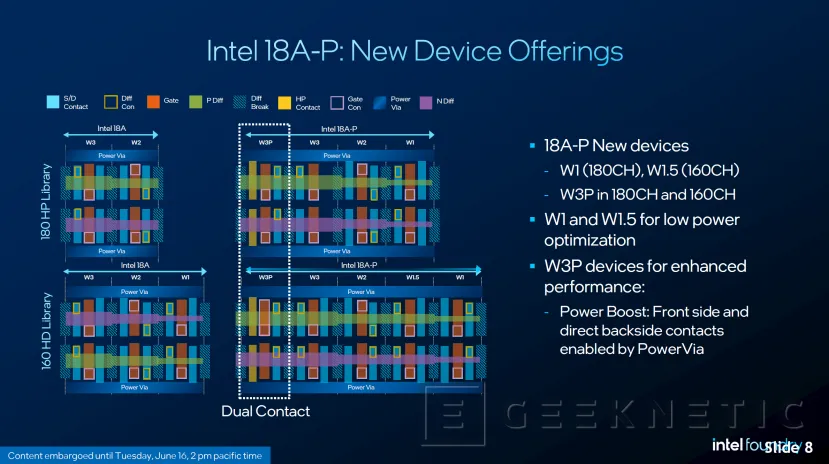
The Intel 18A-P maintains compatibility with the 18A
Another relevant point for customers who want to manufacture their chips with Intel is compatibility with Intel 18A. Intel assures that Intel 18A-P process maintains compatibility with previous node design ruleswhich should make it easier to reuse chips or chip blocks previously designed for 18A, as well as existing libraries and design flows. It also retains the two cell heights of the Intel 18A, 180nm and 160nm.
During the presentation, Intel also reviewed the status of Intel 18A, which is in the phase of increasing production in two factories in the United States. The company claims that The yield, the number of valid chips they obtain per silicon wafer, is ahead of their internal forecastsand that the node is already destined for several client products, with data center solutions planned later. It is a good step forward on the part of Intel in order to strengthen its position as a foundry, both for its own products and to carry out the production of third-party products, thus regaining competitiveness against TSMC and Samsung in advanced processes.
Beyond Intel 18A-P, the company has detailed new metrics on the advantages of combining PowerVia and gate-all-around transistors. According to Intel, these technologies allow the dynamic voltage drop to be reduced by up to 10x and obtain between 5 and 6% more frequency, or more than 15% reduction in dynamic consumption compared to comparable technology with front interconnection. An 11% reduction in routed area is also mentioned, which can translate into more compact designs or more efficient internal routes.