
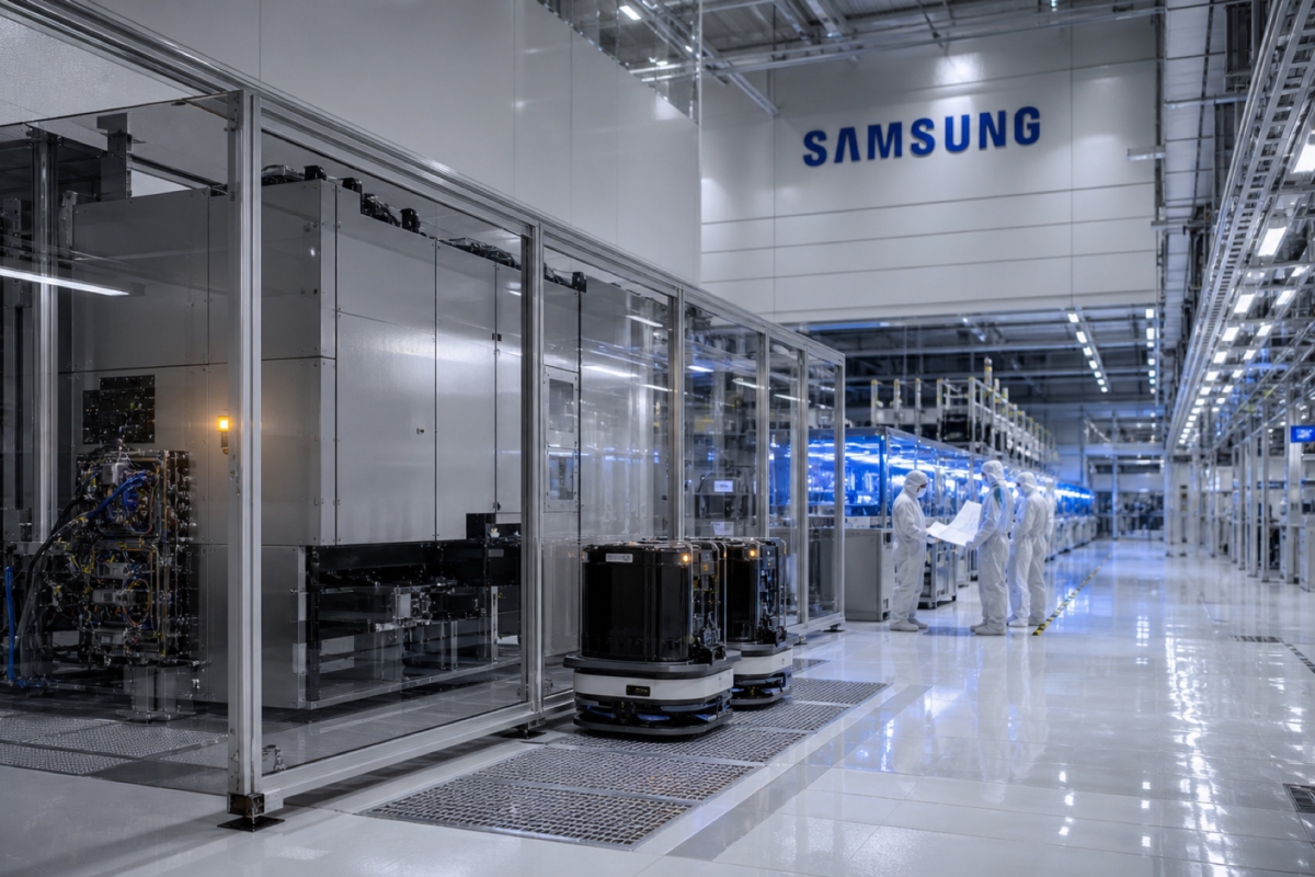
Samsung delays adoption of High-NA EUV lithography until 2030 and its 1nm node
Samsung Foundry has been constantly updating its chip manufacturing machinery in recent years, but there is a specific technological leap that the South Korean company still does not want to make. Although it already has the current generation of EUV lithography, Samsung has not committed to incorporating tools High-NA EUV short-term ASMLand everything indicates that this change will not come until well into the next decade.
As reported by the South Korean media ZDNet Korea, this situation is expected to change with the development of Samsung 1 nanometer nodewhose arrival is scheduled for the year 2030. This would make the company one of the last large manufacturers of cutting-edge semiconductors to incorporate High-NA machinery into its production process, far behind the deadlines managed by its two major rivals in the custom chip manufacturing market.
Intel and TSMC set the pace of adoption
While Samsung takes its time, Intel is already progressively scaling its 14A node towards risk production using High-NA EUV toolsa step that the American company has been preparing for some time as part of its strategy to regain ground against its competitors in advanced manufacturing. For its part, TSMC plans to introduce this same technology in 2029which also places it ahead of Samsung in the adoption schedule of this machinery.
That Samsung is one of the last to get on this bandwagon does not necessarily mean that the company is in a hurry to correct course. In fact, everything indicates that Samsung Foundry is in a comfortable position thanks to the performance you continue to achieve with the Low-NA EUV tools you already have in operationwhich allows you not to depend on an investment that, today, remains enormously expensive.
Why the cost of High-NA machinery matters
To understand Samsung’s decision, it is worth looking at the price of the equipment itself. The most advanced High-NA EUV lithography machine ASML manufactures has a approximate cost of 400 million dollars per unita figure that makes this type of machinery one of the highest investments in the entire semiconductor industry, even for manufacturers the size of Samsung, TSMC or Intel.
Low-NA tools, by comparison, cost about half as muchwhich explains why TSMC has so far chosen to continue scaling nodes and adding improvements generation after generation without making the leap to High-NA, relying on the fact that it can achieve similar competitive advantages with the technology it already masters. Samsung, according to the information available, seems to be following a very similar reasoning to that of its Taiwanese rival.
Multipatterning: the technique that saves time
The key that allows manufacturers like Samsung or TSMC keep squeezing your Low-NA EUV machines without losing too much ground to the competition is a technique known as multipatterning. This process consists of the lithography machine making multiple passes to engrave a design on the same layer of the chip, instead of completing this engraving in a single exposure, as would occur with High-NA machinery.
By performing two engraving passes with Low-NA technology, manufacturers can achieve similar precision benefits as a single exposure with High-NA machinery, significantly reducing the need to purchase new tooling in the short term. However, this technique also has its limits.
A roadmap that fits with Samsung’s plans
Precisely this technical limitation is what explains why the arrival of Samsung’s High-NA machinery is aligned with the 1 nanometer node planned for 2030. According to the information available, This approach is consistent with the roadmap that Samsung Foundry has been communicating in recent months regarding its next manufacturing nodes, in which the company has first prioritized the maturation of nodes such as 2 nanometers and 1.4 nanometers before taking the technological leap of incorporating High-NA lithography into its mass production.
It is important to distinguish at this point what are confirmed plans from what remains, for now, a forecast based on South Korean industry sources. Samsung has not made an official announcement detailing the exact date or conditions for the arrival of its High-NA EUV machinery.so these deadlines should be taken as a reasonable estimate from the company’s known roadmap, and not as a definitive confirmation from the manufacturer.
What this means for the future of advanced chips
To the end user, these types of manufacturing machinery decisions may seem removed from everyday life, but end up directly influencing the efficiency, performance and price of processors and memories who end up assembling computers, smartphones and other electronic devices. The longer it takes a manufacturer to incorporate cutting-edge technology, the more it will depend on optimizing its current processes as much as possible to avoid falling behind the competition.
That Samsung, Intel and TSMC follow such different schedules to adopt High-NA EUV lithography also gives an idea of the different strategies that each manufacturer can follow to reach the same technological destination, something that in the coming years will largely determine which companies manage to maintain the pace of miniaturization that the semiconductor industry has been pursuing for decades.
