
The CSIC opens the largest Spanish infrastructure in Barcelona to manufacture quantum chips
He Higher Council of Scientific Research has inaugurated the Quantum Nanofabrication Area of the White Room from the Barcelona Microelectronics Institute. The new facility is prepared to manufacture and analyze nanoscale structures, devices and circuits aimed at quantum technologies and advanced microelectronics. The CSIC presents it as the largest Spanish research infrastructure of this type.
The remodeling has received a investment of more than 6 million euros. The funds come from PERTE Chip and the Complementary Quantum Communications Planwith European funding from Next Generation EU. The equipment will be available to the national and international scientific and technological community, including companies that need to develop or validate prototypes without having their own clean room.
The most advanced electronic lithography system installed in Spain
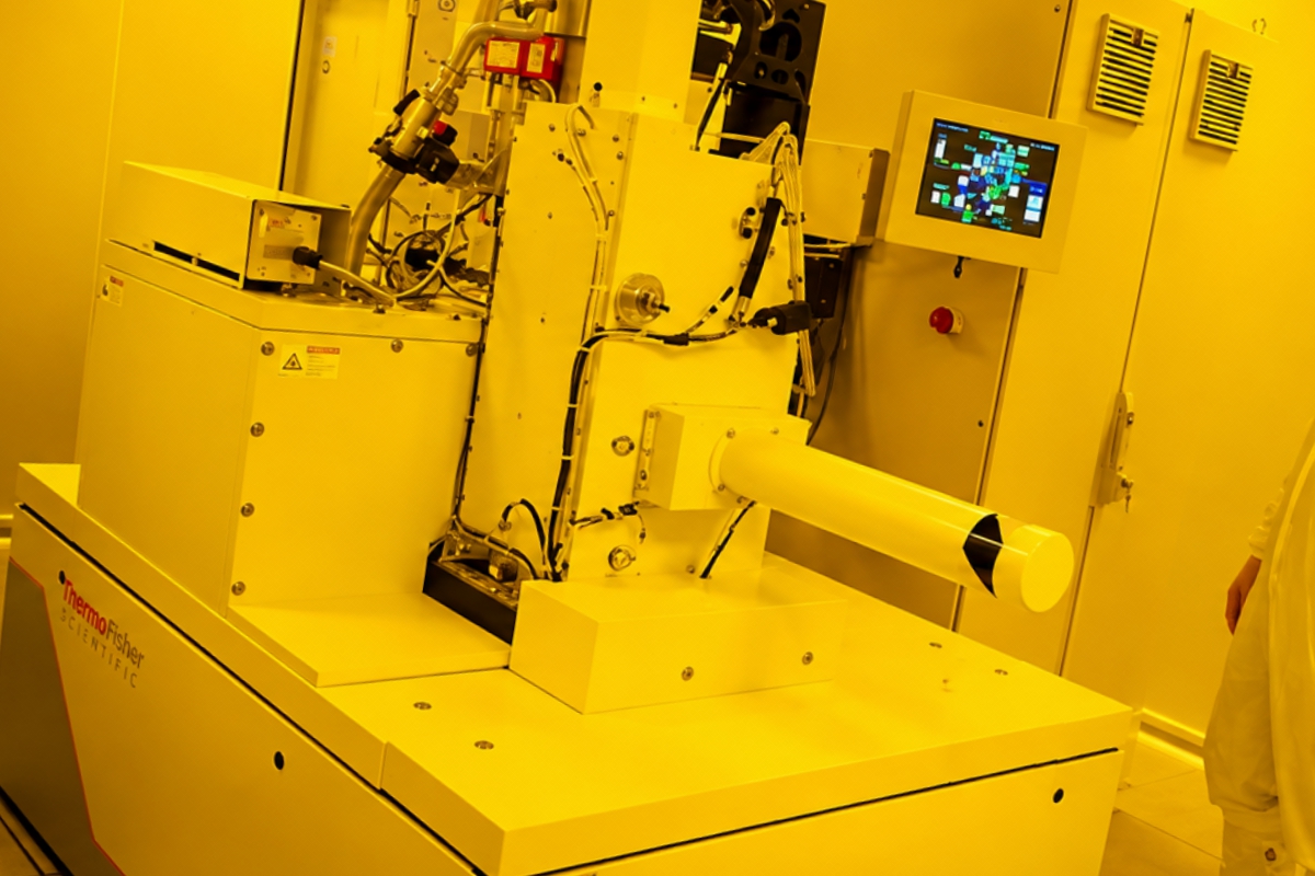
The main piece of the area is a EBPG 5150Plus electron beam lithography system. This technique uses a beam of electrons to directly draw extremely small patterns onto a material prepared for the process. It allows working with geometries that would be difficult to obtain using conventional optical methods and is useful in the development of quantum circuits, photonic components and sensors.
He manufacturer Raith specifies for this family a 100 kV column, beam currents of up to 350 nA and lithography with resolution less than 5 nanometers. It also supports automated wafer and multi-sample exposures, with automatic parameter changes and calibration processes.
The installation incorporates SEM/EBL microscopes and an atomic force microscopeknown as AFM. These equipment allow structures to be inspected during the different manufacturing phases and their characteristics to be measured on a nanometric scale. The ability to create patterns and test results within the same infrastructure reduces dependence on external laboratories during prototype iterations.
A prototype factory for research and companies
The new space should not be confused with a commercial plant dedicated to producing large volumes of semiconductors. Its function is facilitate research, development, characterization and advanced prototyping. Users will be able to test materials, processes and designs before considering broader manufacturing. This shared access is especially important in the quantum field, where the cost of equipment and working conditions make it difficult for each group to maintain its own line.
The area is part of the Micro and Nanofabrication Clean Room of the IMB-CNM and the Micronanofabs Singular Scientific and Technical Infrastructure. The institute accumulates four decades of work in microelectronics design and manufacturing.
The project will have a second phase. The CSIC explains that in the coming months another expansion will begin funded through the Institutional Singulars call, the Department of Research and Universities of the Generalitat of Catalonia and the FEDER program of Catalonia 2021-2027. The institution has not yet detailed which new teams will be incorporated or the complete schedule for that performance.
From the design of a device to its possible industrial use
The availability for researchers and companies attempts to cover one of the most difficult steps in technology transfer: convert an experimental design into a device that can be manufactured, measured, and its results repeated. In quantum technologies, a minor variation during manufacturing can alter the behavior of the component. Having high-precision lithography and metrology in an accessible facility allows processes to be compared and designs corrected before moving to another scale.
The CSIC relates this capacity to future applications in quantum computing, secure communications, sensors, energy and medical devices.
It also complements other quantum initiatives developed in Spain. The Barcelona Supercomputing Center hosts quantum systems integrated with MareNostrum 5, while the IMB-CNM focuses here on the manufacturing and characterization of the devices. They are different tasks within the same technological chain: one infrastructure executes workloads and the other allows research on how to build components.
QuARC-CSIC will coordinate 36 research groups
The inauguration It is part of the Quantum Science and Technologies Strategy presented by the CSIC. Within it, QuARC-CSIC has been created, the Center for Quantum Science and Technologies that will bring together capabilities distributed across different centers. Its physical headquarters will be in Madrid, although it will work with institutes from other communities, including the IMB-CNM.
QuARC-CSIC will rely on the QTEP-CSIC Interdisciplinary Thematic Platformwhich brings together 36 research groups belonging to 21 institutes distributed in nine autonomous communities. Its objectives include opening lines of work, coordinating national and international collaborations, facilitating technology transfer and supporting business creation.
The new Barcelona area provides this structure with a specific physical capacity: manufacturing and measuring devices with nanometric precision within Spain. After the investment of more than 6 million euros, the next relevant data will be the number of public and private projects that use the facility and the prototypes that manage to pass the laboratory phase.
