
Samsung stacks transistors in 3D to make smaller, more efficient chips
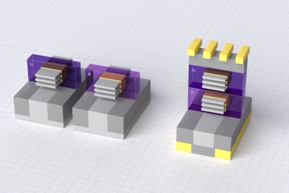
Samsung has announced a breakthrough in transistor design that could mark a before and after in chip manufacturing. The South Korean company has developed a architecture called 3D Stacked FETwhich consists of placing two different types of transistors on top of each other instead of arranging them side by side, as has traditionally been done.
The change may seem simple on paper, but it involves solving several technical problems at once: power delivery, uniformity during manufacturing and electrical interference between layers. According to Samsung, its team has managed to overcome these obstacles, which opens the door to smaller, denser chips with significantly higher performance than current solutions.
A featured proposal at the VLSI 2026 Symposium
Samsung Electronics presented this technology in an article titled “First Demonstration of 42nm Gate Pitch 3D Stacked FET Transistors Incorporating Triple Stacked Nanosheet Channels for Advanced Logic Applications”exhibited at the VLSI Symposium 2026.
The work did not go unnoticed among the technical community: it was selected as the best article among more than a thousand proposals submitted, with a score of 8.29 out of 10. Additionally, it was included among the technical highlights of the conference and appeared in the event’s official press kit, giving an idea of the interest it has generated within the semiconductor industry.
The VLSI Symposium is one of the leading technical forums in the sector, where researchers, scientists and engineers share advances related to very large-scale integration and the technologies that will define the next manufacturing nodes.
Why stacked transistors are the next frontier
For decades, semiconductor manufacturing has advanced by reducing the size of transistors to fit more units on the same silicon surface. This strategy has allowed us to improve both the performance and energy efficiency of the chips, but it has a physical limit.or: There comes a point where you can no longer reduce the size of each individual transistor without electrical problems appearing.
Over the years, architectures have evolved: from planar transistors moved to FinFETs and, more recently, to the envelope gate transistors (GAA). Despite these changes, transistors have continued to be placed, for the most part, next to each other on the same two-dimensional plane.
Samsung’s proposal breaks with that scheme. Its architecture vertically stacks two types of transistors, n-type and p-typewhich significantly reduces the space required inside the chip. Instead of continuing to shrink each component, the company proposes making better use of vertical space.
How Samsung has solved the main challenges
Stacking transistors vertically is not trivial. Samsung explains that it has addressed the problems associated with this architecture through three specific solutions:
- The use of triple layer stacked nanosheet channelswhich guarantee sufficient current flow through a much more compact structure.
- The application of advanced epitaxial growth technologywhich allows creating smooth and defect-free layers so that electrical signals circulate stably.
- The development of an insulating structure called Medium Dielectric Insulation (MDI)responsible for separating both layers of transistors without affecting their performance.
With these three pieces, the company claims to have achieved a functional and stable architecture, not just a theoretical concept.
A 42nm gate pitch as a proof of concept
Samsung has demonstrated this technology using a 42nm gate pitcha measurement indicating the distance between the gates of adjacent transistors. This result is relevant because it suggests that the 3D stacked FET architecture could be applied to the most advanced manufacturing nodes that currently exist in the industry.
The company has also evaluated the uniformity of technologycomparing the electrical characteristics of several structures within the same wafer. According to the results obtained, the properties remained consistent between the different samples analyzed, which reinforces the viability of manufacturing this architecture on a larger scale.
What would this change mean for the chips of the future?
If this technology is produced on a large scale, it would represent a fundamental change from the planar designs that have dominated the industry for years: the leap towards a truly three-dimensional transistor architecture. This approach could result in chips with much higher transistor density, better overall performance, and higher power efficiency than current GAA-based solutions.
At the moment, Samsung has not provided a specific date for when this technology could be commercialized or when it would be used in mass-produced products. For now, it is a technical demonstration that lays the foundations for what could be the next great transition in semiconductor design, in a field where manufacturers such as Samsung, TSMC and Intel compete to lead the most advanced process nodes.
