
SK hynix makes a leap in DDR5: the new 3 GB A-die AKBD chip aims at 7200 MT/s and takes over from the M-die
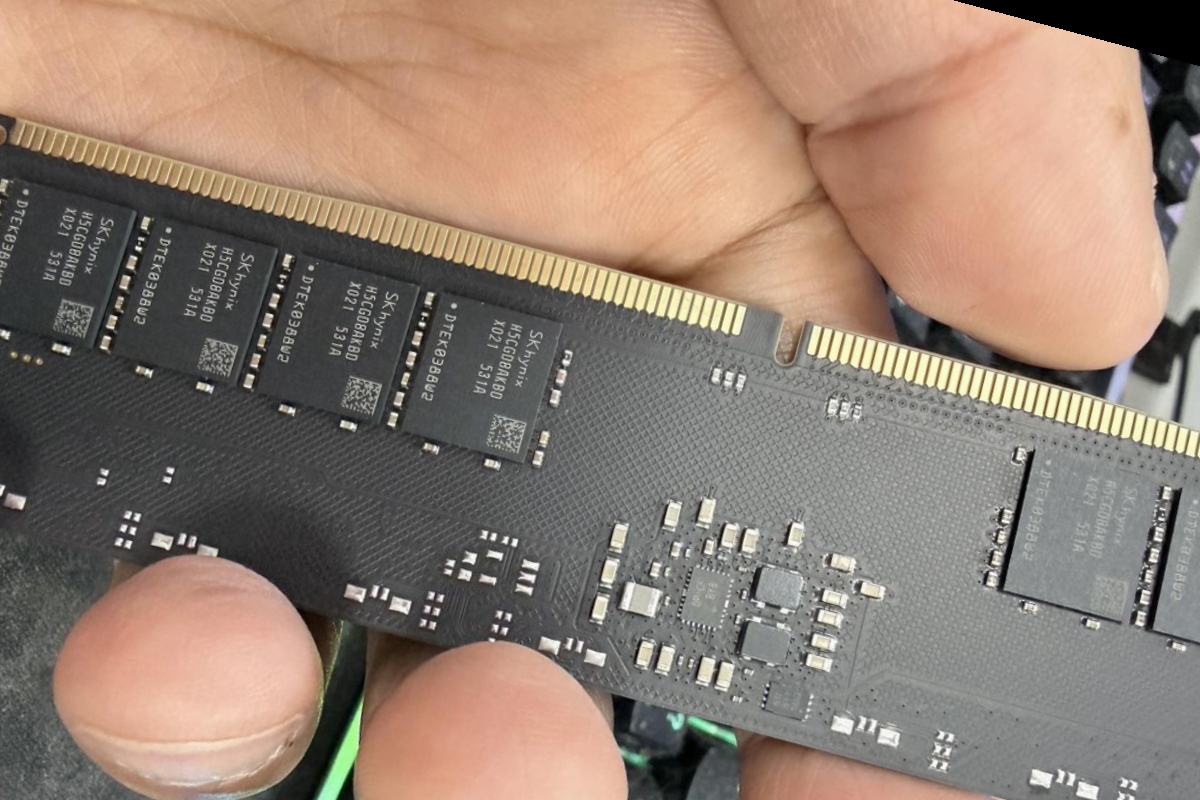
Leaks with first and last names are usually the most interesting because they allow you to read between the lines. A DDR5 module with X021 silkscreen and AKBD code has appeared in photos shared by Kevin Wu (Team Group). The clue that completes the puzzle is provided by @unikoshardware: it would be the new second generation 3GB A-die from SK hynix, the natural successor to the M-die that dominated the first stage of DDR5.
From EB to KB: how to read the “AKBD”
SK hynix has been quite consistent in its internal labels. The EB, FB, GB or HB terminations have been marking steps in native JEDEC frequency: 4,800, 5,600, 6,000/6,200 and 6,400 MT/s, respectively. If the new chip looks “KB”, the most reasonable interpretation is 7,200 MT/s base. This is not an artificially elevated XMP/EXPO profile, but rather an indication of what the silicon can sustain within the standard specification, at conservative voltages and timings.
3 GB density per chip: what it means for capacity
let it be talked about 3 GB per IC It is not a whim: it conditions the topology of the modules. In DDR5, the usual are 2 GB and 4 GB. At 3 GB, a 16-chip DIMM offers 48 GB; with 8 chips, 24 GB. This fits with the rise of 2×24 GB (48 GB) and 2×48 GB (96 GB) kits that we have already seen with M-dieproviding a sweet spot between capacity and latency compared to the populist 2×32 GB. If the new A-die inherits the good behavior of M-die with intermediate densities, we could see 2×24 GB kits at 7,200–7,600 MT/s stable with reasonable profiles without the need for aggressive voltage escalations.
8-layer PCB in the sample: a ceiling for overclocking… and a message to the market
The leaked unit mounts 8-layer PCB. It’s enough to nail 7,200 MT/s JEDEC and somewhat more cheerful profiles, but it’s not the ideal terrain for extreme overclocking above 8,000 MT/s. To do this, manufacturers typically move to 10 or 12 layers, which improve the signal integrity, crosstalk between lines, and power distribution of the PMIC.
DDR5 has learned through iterations that more MHz does not always mean better effective latency. The key is in the tRFC, tFAW, tRCD and tCCD_L that the XMP/EXPO profiles set to match frequency and stability. M-dies already demonstrated that they could sustain CL34–36 at 7,200–7,600 with 1.35–1.40 V in well-binned kits. If the A-die AKBD scales equally or better, we will see 7,200 JEDEC profiles with relaxed timings for universal compatibility and, in parallel, XMP profiles with more aggressive latencies in the enthusiast ranges.
PMIC, temperatures and the other half of performance
The stability of a DDR5 module no longer depends only on the IC; the PMIC on-DIMM and the thermal system (sink, pads, airflow) play an equally decisive role. At 7,200–7,800 MT/s, the PMIC works with more demanding current transients; If SK hynix has optimized the A-die consumption curves, the modules will be able to maintain high frequencies during sustained loads without silent “thermal throttling”. Hence, many premium kits combine these chips with higher mass heatsinks or even bars with heat pipes, not for aesthetics, but to stabilize thermal variations that alter the signal.
Why SK hynix now dominates where Samsung once reigned
In DDR4, saying “B-die” was synonymous with low latencies and clean scaling; overclockers turned it into a religion. With DDR5, Samsung lost that halo due to a combination of process, driver maturity, and, above all, the speed with which SK hynix fine-tuned its M-die. If the second generation A-die is confirmed as a silicon that raises the base to 7200 and maintains a favorable voltage curve, SK hynix will consolidate a leadership that, at this point, no longer seems temporary.
What to expect in the short term
The most sensible thing is to anticipate 2×24 GB and 2×48 GB kits at 7,200–7,600 MT/s as the first batchwith 8-layer PCBs for volume and a price close to the current mid-high ranges. From there, we will see editions with 10/12 layers and more ambitious XMP profiles to cross 8,000–8,200 MT/s with stability on new generation Z boards.
The AKBD A-die is not intended to break validation records; aims to make 7,200 MT/s the new floor for premium consumer memory. If you add to that base well-designed kits, PCBs with more layers when necessary and mature firmware on boards and CPUs, the result is an ecosystem where bandwidth is no longer the bottleneck and effective latency is once again the battlefield. SK hynix already has inertia in its favor; If this chip does what its label suggests, the dominance in DDR5 will continue to expand, and the user will gain something that is often forgotten: predictability. Open the box, mount, load XMP and you’re done.